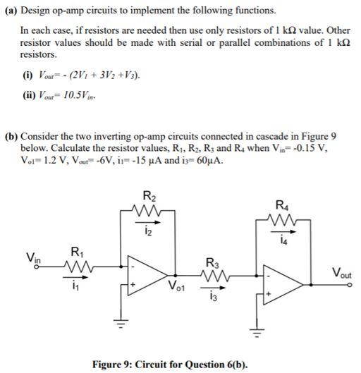
amp circuits to implement the following functions Circuit Diagram DESIGN EXAMPLE OF A TWO-STAGE OP AMP Example 23-1 - Design of a Two-Stage Op Amp If K N'=120µA/V2, K P'= 25µA/V2, V TN = |V TP | = 0.5±0.15V, N = 0.06V-1, and P = 0.08V-1, design a two-stage, CMOS op amp that meets the following specifications. , =. =) = /) 3 (/) =--+ (/) =

the op amp's place in the world of analog electronics. Chapter 2 reviews some basic phys-ics and develops the fundamental circuit equations that are used throughout the book. Similar equations have been developed in other books, but the presentation here empha-sizes material required for speedy op amp design. The ideal op amp equations are devel- The circuit operates from a dual supply +Vcc and -Vee which ensures a constant supply. The voltage that appears at the output, Vout of the amplifier is the difference between the two input signals as the two base inputs are in anti-phase with each other. So as the forward bias of transistor, TR1 is increased, the forward bias of transistor TR2 is reduced and vice versa.
Ultimate Guide to Op Circuit Diagram
Operational amplifiers (op amp) are linear devices that have all the properties required for nearly ideal DC amplification and are therefore used extensively in signal conditioning or filtering or to perform mathematical operations such as adding, subtracting, integration, and differentiation. The purpose of this article is to present 10 basics circuits for newcomers to electronics designs and Operational Amplifier Circuits as Computational Devices So far we have explored the use of op amps to multiply a signal by a constant. For the inverting amplifier the multiplication constant is the gain R2 − R1 and for the non inverting amplifier the multiplication constant is the gain R2 1+ R1. Op amps may also perform other

Lecture 8: Op-Amps; About this Video. Circuit design is complicated by interactions among elements, but these interactions can be reduced or eliminated by using an op-amp as a buffer. This lecture covers how to analyze and design op-amp circuits. Lecture handout (PDF) Lecture slides (PDF) Recitation Video One of the most famous of these was the LM741 op-amp. You still see many circuits using this op-amp. Fortunately, manufacturers kept the pin layouts the same for the ever-increasing and improving range of op-amps. Because the external feedback components largely determine the behavior of op-amp circuits, you can generally substitute other op-amps. An op-amp has two inputs, an inverting terminal (labeled „-") and a non-inverting terminal (labeled „+"). And has a single output. The first input is called inverting because the output voltage is inverse of the voltage applied at the inverting input, times the gain of the amplifier circuit.If we apply the signal to the non-inverting input we get the same signal on the output, times gain.